Shop a wide selection of FEI Company Helios NanoLab DualBeam's on LabX. Find new and used pricing to meet your lab needs. Choose from top brands in our marketplace.
FEI Company Helios NanoLab DualBeam
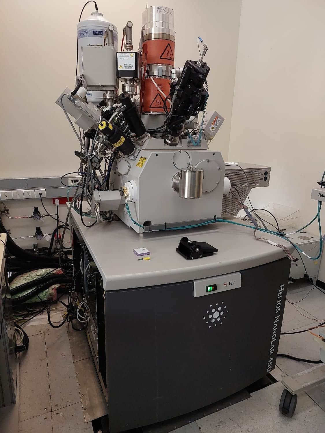
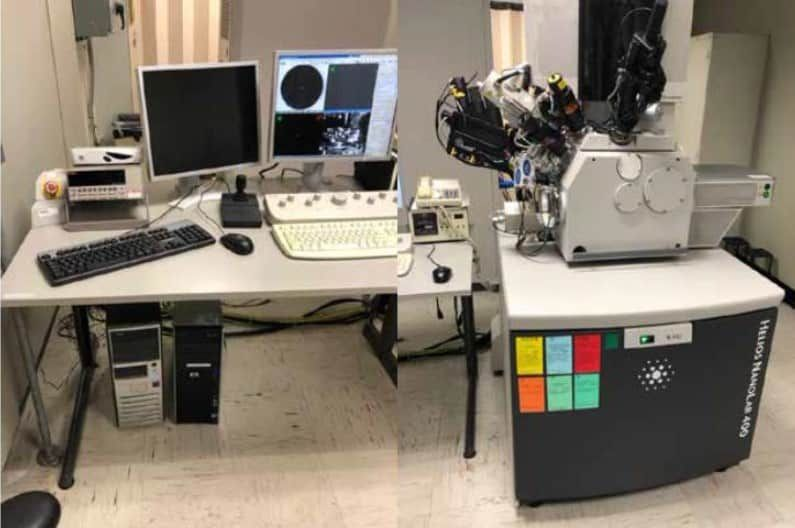
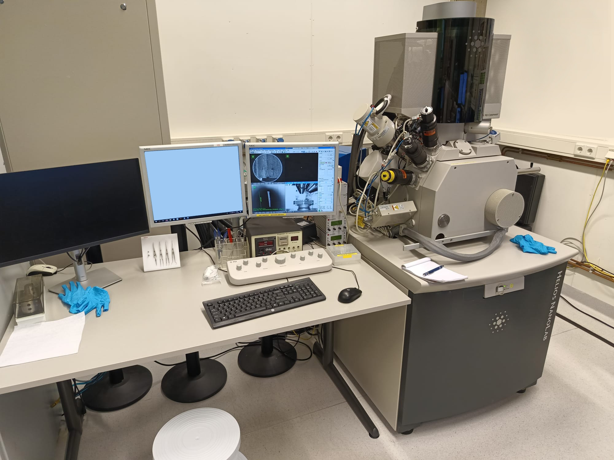
Imaging, analysis and control of matter at the nanoscale — keys to future research and development — are routine with the Helios NanoLab™ 50 series DualBeam™ . This SEM/FIB combines the most advanced scanning electron microscope (SEM) and focused ion beam (FIB) technologies with innovative gas chemistries, detectors and manipulators. Featuring unsurpassed SEM resolution, image quality and stunning Tomahawk™ FIB performance, imaging, milling or preparing samples is fast and easy for semiconductor and data storage labs, research facilities and industrial applications.
Helios NanoLab 450S
The Helios NanoLab 450S is ideally suited for high throughput, high-resolution S/TEM sample preparation, imaging and analysis. Its exclusive FlipStage and in-situ STEM detector can flip from sample preparation to STEM imaging in seconds without breaking vacuum or exposing the sample to the environment.
Helios NanoLab 600i
The Helios NanoLab 600i builds on the success of FEI’s winning DualBeam series offering advances in the ion beam, electron beam, patterning and a range of features to make milling, imaging, analysis and sample preparation down to a nanoscale, standard applications in the lab.
Helios NanoLab 650
The Helios NanoLab 650 features FEI’s most recent advances in field emission SEM (FESEM) and focused ion beam (FIB) technologies and their combined use. As FEI’s 11th DualBeam platform, it is designed to access a new world of extreme high resolution (XHR) 2D and 3D characterization, 3D NanoPrototyping, and higher quality sample preparation.
Helios NanoLab 1200
The Helios family also includes the Helios NanoLab 1200, a full 300 mm wafer platform providing unmatched performance for larger samples where the need to maintain wafers intact is critical. FEI’s industry leadership in full wafer DualBeam technology now benefits from advanced electron and ion optics to bring unprecedented resolution to full wafer TEM (transmission electron microscope) sample preparation, defect characterization, and failure analysis.
Filter By
Price Range
Listing Type
Condition
Category
Manufacturer
Become a member and enjoy exclusive benefits
Create an account now for exclusive benefits, personalized recommendations, and seamless order tracking. Elevate your lab experience today!


